There’s more to those lines on the circuit diagram the meet the eye…
My name is Chiba Hiroki and I work in the Solutions Development team. In this column, I discuss my experiences with devices I have worked with.
While the circuit diagram is an important (in fact indispensable) element of device design, in this article I will explain why a perfect schematic will not guarantee that your device will meet performance requirements.
When a device modified to conform to an amendment to a standard does not function properly
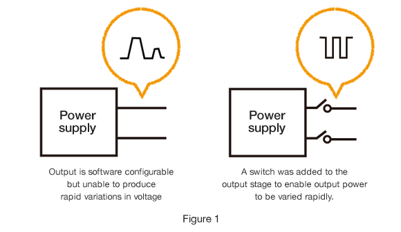
The device I worked on tested variations in power supply, and was able to vary its output voltage in a split second via a software-controlled switch fitted to the power supply output. While the power supply in question did have a built-in function for varying output voltage in accordance with software settings, it was unable to deliver the extremely rapid changes in voltage required to perform the voltage variation tests that are part of some standards. We therefore enabled the device to be compatible with these tests by flipping a switch added to the output stage (see Figure 1).

Kikusui had been producing the device in question since before I joined the team. The client had requested that we make the device compatible with a recent amendment to the standard. As only a minor amendment was anticipated, we decided to modify the circuitry of the existing device, while keeping the component layout more or less unchanged. A few weeks later the modified device was ready. Now all that remained was to turn it on…
When we turned the device on, however, we found that when the device was operated in accordance with the new standard, the device’s output waveform exhibited distortions, including a larger voltage “undershoot” upon power-off than was observed before modification. In an attempt to narrow down the possible causes, we then tried operating the device on the conditions prescribed in the old standard. This time, the device performed to the same standard as the previous device. So why was the undershoot in voltage more pronounced under the new testing conditions?
Parasitic inductance
While the new standard did not change the allowed variation in power supply voltage, it did call for a much lower load resistance of only a few ohms, down from several hundred kiloohms under the previous standard. In other words, the load current increased.
The test involved rapidly switching the circuit off under significant load current. While the change in voltage was the same as that used in the previous standard, the change in current was now much larger. This meant that the increased magnitude of the variation in current resulted in the induction of a larger parasitic inductance component (an induced electromotive force that does not appear on the schematic) which affected the circuit.
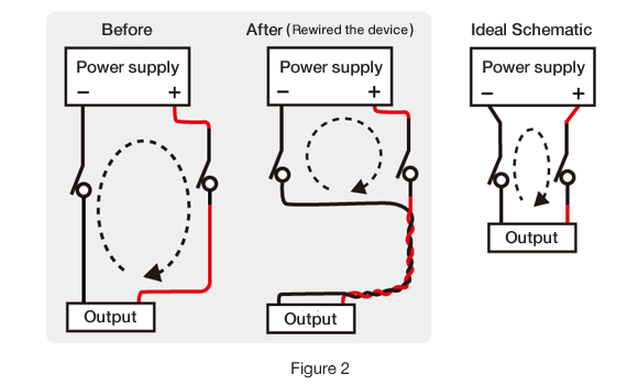
Furthermore, upon inspecting the positions of the components and wires within the device, we found that components connected to the supply line were far removed from the components connected to the ground line, and also that the circuit featured long wires on the positive side that were situated far away from the wires on the negative side, with the wires arranged in a large loop. This poor design was exacerbating the parasitic inductance.
How to contain an invisible enemy
Now that we knew the cause of the problem, all that remained was to fix it. First, we tweaked the switching speed, which had been configured to outperform the speed required under the standard by an unnecessarily large margin.
Next came the wiring loop. While ideally we would have brought the components closer together and connected them using wires that were as short and thick as possible (in order to make the loop smaller), repositioning components would have been very time-consuming so we decided against this. Instead, we decided to rewire the device. Luckily, this device was connected using cables rather than tracks on a PCB, so we were able to perform an on on-the-spot repair in which we shortened the wires and twisted the ground and supply wires together, thereby reducing the size of the induction loop and significantly reducing the effects of parasitic impedance. Ultimately, we were able to achieve performance equivalent to that before modification (see Figure 2).

The “invisible demon” that lurks in the circuit
As many will be aware, electronic circuits are home to unintended resistance, capacitance and inductance components, referred to as the “parasitic” and “stray” component. However, these components often do not materialize until power is actually turned on. While circuit simulators that attempt to model these dynamics do exist, I don’t think the technology is “quite there” yet.
The case above required a quick solution. As such, the solution we implemented was not the optimum one and contains room for improvement. However, this was a good lesson for me, because it made me realize that what appears as just a regular wire on a schematic may in fact be an important factor in defining the characteristics of a device.
This experience taught me the importance of considering how changes to a specification will actually affect a circuit. It also made me further appreciate the importance of predicting in advance not only how a circuit will operate but also what parasitic components will be generated as a result of the position of components and wires.
In conclusion, whenever you modify a circuit, always assume that an invisible “demon” may be lurking inside it!


